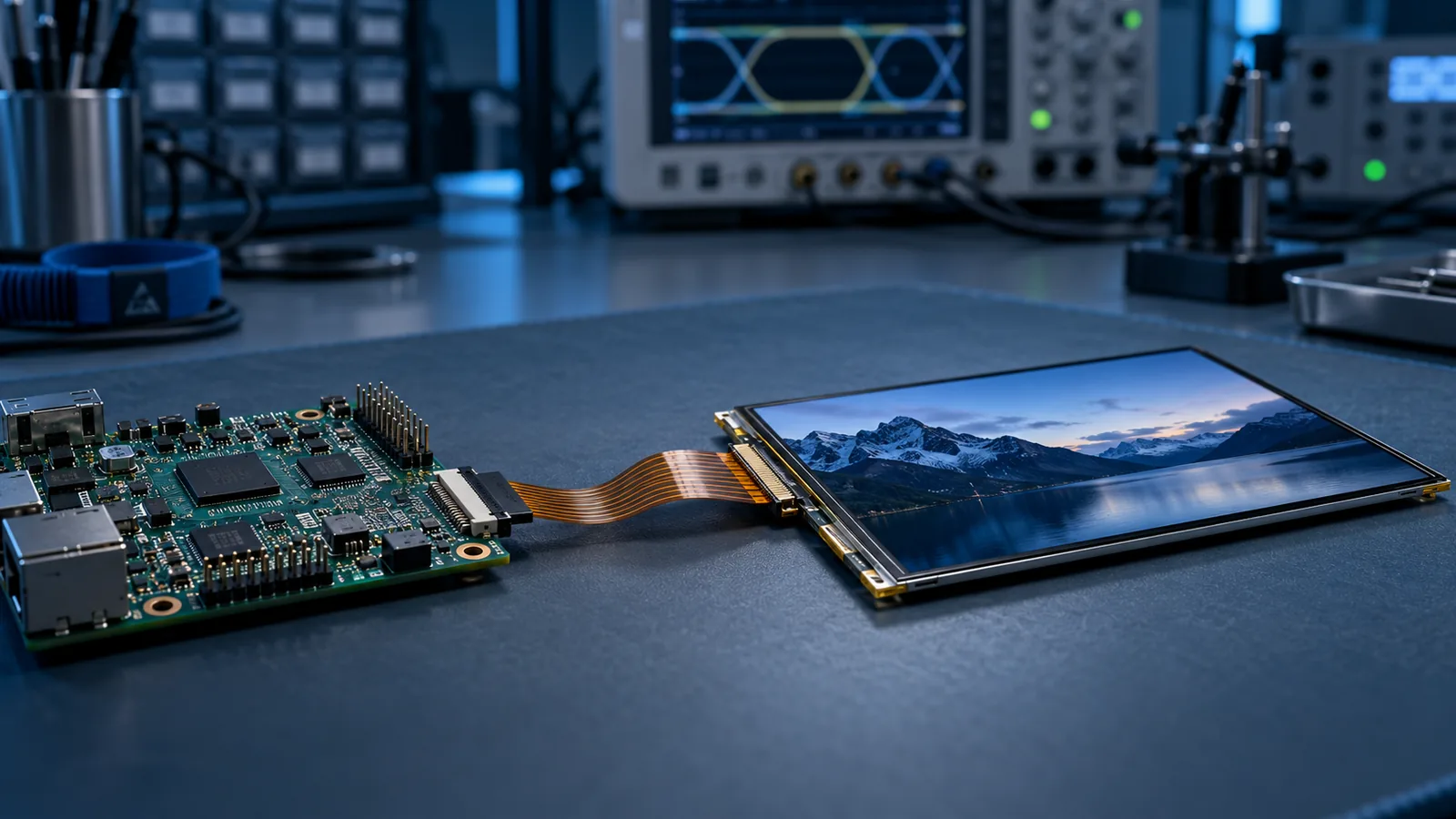
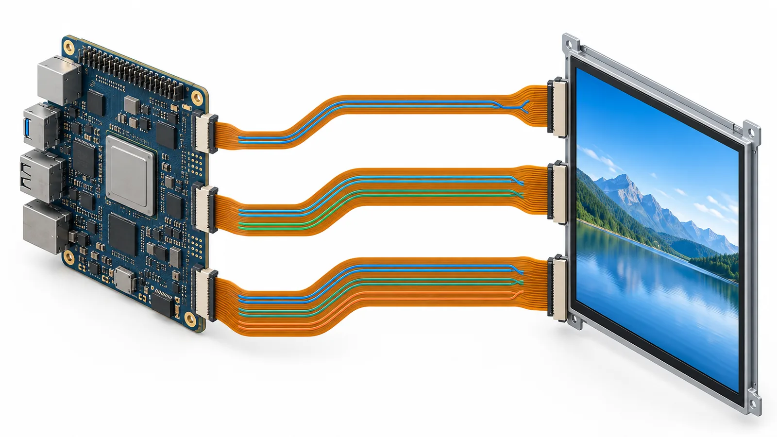
MIPI DSI reduces display pin count by packetizing image and control data over a high-speed serial link. Common embedded implementations use one, two or four data lanes plus a clock lane, although the options are device-specific. A panel marked “4-lane MIPI” cannot automatically be driven with two lanes, and a host with four available lanes cannot force a panel to accept four.
Lane selection is therefore a compatibility decision before it is a bandwidth optimization. Confirm the exact display mode, initialization sequence, pixel format and D-PHY limits on both endpoints. If the system interface is not fixed yet, begin with the broader TFT LCD interface comparison.
The short answer
Use the lowest lane count that both endpoints explicitly support and that can carry the required stream with qualified timing margin. Fewer lanes save pins and routing but raise the required rate on every lane. More lanes reduce the rate per lane but add high-speed pairs, routing constraints and endpoint configuration requirements. Neither choice is universally better.
Eight inputs required before calculating lanes
| Input | Why it matters |
|---|---|
| Active resolution | Defines the number of visible pixels in each frame. |
| Target frame rate | Determines how often the pixel payload must be delivered. |
| Pixel format | RGB565, RGB666 and RGB888 carry different payload bits per pixel. |
| Video or command mode | Changes how pixels, blanking and control traffic use the link. |
| Video-mode packetization | Burst and non-burst modes use line time differently. |
| Panel lane options | The receiver may require a fixed lane count or initialization setting. |
| Host lane and PLL limits | The transmitter must generate a supported per-lane rate and timing. |
| FPC, connector and PCB path | Loss, skew and discontinuities affect signal margin at the selected rate. |
Start with active pixel payload
The active-image payload is a useful lower-bound calculation:
This is not yet the final high-speed lane rate. DSI packets include protocol overhead, and video timing may include blanking or null-packet behavior. The host controller may also impose specific byte-clock, PLL-divider or horizontal-timing relationships. Use the host vendor’s DSI calculation method and the panel timing table for the final value.
Worked lower-bound examples
An uncompressed 800 × 480 image at 60 fps and RGB888 has an active payload of:
Before protocol and blanking allowance, that equals 276.48 Mbit/s per lane on two data lanes or 138.24 Mbit/s per lane on four. A 1280 × 800 RGB888 stream at 60 fps has an active payload of 1,474.56 Mbit/s, or 368.64 Mbit/s per lane across four lanes. These examples are arithmetic only; they do not establish a valid configuration for any specific panel.
Why the final lane rate is higher than active payload
Video-mode DSI converts a parallel display-timing concept into packets. Depending on burst or non-burst operation, the link can carry synchronization packets, blanking packets or null packets around active pixel data. Packet headers, checks and required transition time also consume link time. In command mode, pixel updates, addresses, commands, acknowledgements and tearing-effect synchronization shape the transfer window.
Do not apply one universal overhead percentage to every design. Instead, start with the panel’s required mode and timing, configure the horizontal and vertical totals, and use the DSI host documentation or clock calculator to determine the necessary high-speed clock. Then verify that the result is within the transmitter and receiver ranges at every required operating condition.
Video mode, command mode and lane choice
Video mode
Video mode continuously transfers frames according to display timing. Non-burst operation preserves more of the incoming timing structure on the serial link. Burst mode sends active pixels in a time-compressed burst and can leave a larger interval for low-power operation or other link activity when both endpoints support the configuration.
Command mode
Command-mode panels typically accept commands and pixel writes into display memory. Average UI activity may be low, but the lane configuration still has to deliver the largest required update inside the available time. Partial updates can reduce traffic; full-screen animation or short update windows can restore a high peak-rate requirement. Confirm DCS commands, address windows, tearing-effect behavior and maximum write rate.
A lane count suitable for a mostly static menu may not meet a later requirement for smooth full-screen animation. Define the real update behavior before releasing hardware.
Match host and panel capabilities
- Lane count: identify the exact supported combinations at both endpoints.
- Lane mapping and polarity: follow the permitted connector and PCB mapping rules; do not assume every implementation supports swaps.
- Per-lane HS range: the calculated rate must be above the required minimum and below the allowed maximum for both host and panel.
- Clock behavior: confirm continuous or non-continuous clock requirements and transition timing.
- PHY revision and timing: program the host using its documented D-PHY timing values rather than copying registers from another panel.
- Pixel format: the DSI packet format, panel setting and application framebuffer must agree.
- Initialization: obtain the exact reset, sleep-out, display-on and vendor command sequence for the panel revision.
Fewer lanes versus more lanes
| Choice | Potential advantage | Risk to verify |
|---|---|---|
| Fewer data lanes | Fewer FPC and host pins; simpler pair count. | Higher rate per lane, tighter loss/jitter margin and possible host/panel rate-limit conflict. |
| More data lanes | Lower rate per lane for the same payload. | More differential pairs, lane-to-lane timing, connector pins and configuration dependencies. |
| Higher frame rate or color depth | Smoother motion or more color information. | Higher payload, memory traffic and PHY rate. |
| Compression where supported | Reduced transport bandwidth. | Both endpoints and the complete software stack must support the same compression mode. |
PCB, FPC and industrial system constraints
Each D-PHY data lane is a high-speed differential pair. Maintain the impedance and routing geometry required by the host, panel and stack-up; keep the two conductors of a pair tightly coupled and avoid stubs. Minimize unnecessary connectors, vias and layer changes. Route over a continuous reference structure and keep switching power nodes away from the display link.
Protection devices and common-mode components are not transparent at high speed. Select parts with characteristics suitable for the required lane rate and validate the complete path, including connector launches and FPC. If the TFT tail needs modification, use the custom TFT LCD FPC guide to freeze pair mapping, geometry and the controlled drawing.
Industrial equipment adds temperature range, power noise, cable routing, radiated immunity and long service expectations. A room-temperature development board on an open bench is not the production channel. Test the final PCB, FPC, enclosure, grounding and nearby loads.
A practical lane-selection workflow
- Freeze the panel model and obtain its current DSI timing and initialization documents.
- List the lane counts, video/command modes, formats and HS-rate range supported by the panel.
- Do the same for the host DSI controller and D-PHY.
- Calculate active payload from resolution, frame rate and bits per pixel.
- Model packetization, blanking and transition requirements using the exact operating mode.
- Select a shared lane count and valid per-lane rate with implementation margin.
- Program PLL, byte clock, D-PHY timings, packet format and initialization sequence from the host documentation.
- Validate the complete physical channel and software sequence across operating corners.
Validation before design release
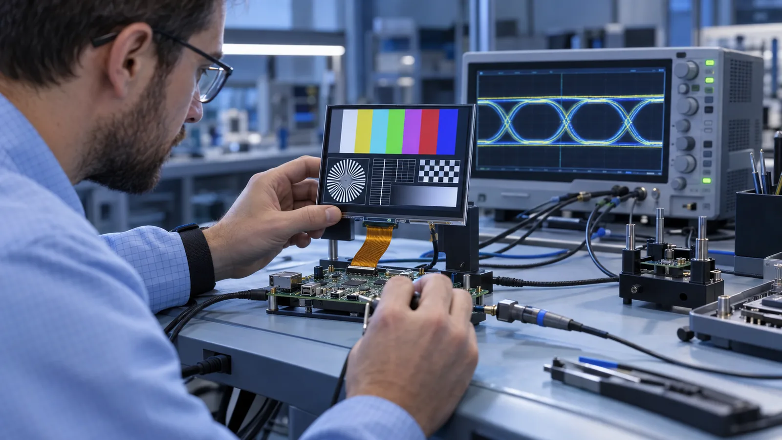
Begin with reset, power sequence and low-power command exchange, then confirm the transition into high-speed transmission. Use solid colors, ramps, checkerboards and moving content to expose pixel-format, mapping and intermittent link faults. Exercise the maximum intended update rate and concurrent system workloads.
For electrical validation, use test fixtures and measurement equipment appropriate to the D-PHY rate. Casual probing can load the pair and create or hide failures. If the host provides PHY or protocol status, capture timeout, contention, ECC, CRC and lane-state information during bring-up. Repeat cold start, warm operation, voltage limits and required EMC tests.
Common selection mistakes
- Choosing lane count from resolution alone.
- Using active-pixel payload as the final HS rate without packet or timing analysis.
- Assuming a four-lane panel can be configured for one or two lanes.
- Copying PHY timing registers from a different processor, panel or lane rate.
- Ignoring the panel’s initialization commands or command/video mode requirement.
- Testing a short development FPC and releasing a different production interconnect.
If the link does not start reliably, use the industrial TFT LCD interface troubleshooting guide to separate power, reset, protocol, timing and signal-integrity faults.
What to send for a MIPI display review
- Exact panel model, datasheet, DSI timing table and initialization code.
- Host processor or bridge part number and software platform.
- Resolution, frame rate, pixel format and update behavior.
- Required video or command mode and supported lane counts.
- Calculated lane rate, PLL/clock plan and D-PHY timing configuration.
- Connector pinout, PCB stack-up, FPC route and protection components.
- Operating voltage, temperature and EMC requirements.
For a verified module example, review the DS-T078VYRA-01 7.8-inch 400×1280 4-lane MIPI TFT. Confirm its current documents and host compatibility before design-in.
Technical references
- MIPI Alliance — Display Serial Interface (MIPI DSI): official DSI overview, protocol context and D-PHY relationship.
- MIPI Alliance — MIPI D-PHY: official physical-layer overview and scalable data-lane architecture.
- NXP — i.MX 8/RT MIPI DSI/CSI-2 (AN13573): DSI architecture, packet concepts and video-mode timing examples.