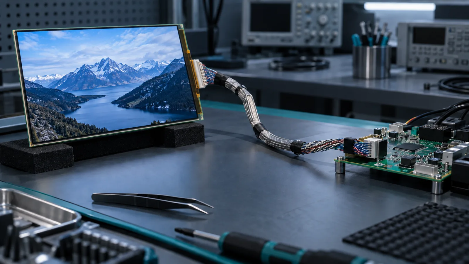
“Will a 300 mm LVDS cable work?” sounds like a length question, but the engineering answer depends on the complete link. Pixel clock, serializer mapping, cable loss, differential impedance, skew, connector transitions, grounding, shielding and receiver margin all contribute. A cable that works on one panel may fail on another even when the diagonal size and connector look similar.
First confirm that the module actually uses an LVDS/OpenLDI-type panel interface. Then verify the host output and the display’s channel count, mapping and timing. The broader TFT LCD interface guide explains how LVDS differs from parallel RGB, MIPI DSI and MCU interfaces.
The short answer: use the minimum practical length
Route the cable using the real enclosure, PCB positions, connector orientations, bend radius and assembly process. Add only the service allowance needed for installation and strain relief. Unused loops do not create useful margin; they add insertion loss, coupling area and opportunities for poor routing.
Seven inputs that determine the usable length
| Input | Why it matters | What to obtain |
|---|---|---|
| Pixel clock and link rate | Higher edge and symbol rates leave less loss and jitter margin. | Panel timing table and source configuration. |
| Single- or dual-channel link | Channel count changes pair count, mapping and inter-channel timing requirements. | Exact panel LVDS definition. |
| Cable construction | Impedance, attenuation, pair balance and skew are properties of the assembly, not its length alone. | Cable drawing and electrical specification. |
| Connectors and adapters | Each transition can introduce impedance discontinuity, added loss and crosstalk. | Mating connector data and the full signal path. |
| Ground and shield strategy | Common-mode current and shielding affect immunity and emissions. | Chassis, signal-ground and shield termination plan. |
| Installation environment | Motors, relays, DC/DC converters and radio transmitters can reduce system margin. | Final cable route and nearby noise sources. |
| Production and temperature variation | A room-temperature prototype is only one operating point. | Required voltage, temperature and manufacturing corners. |
Why increasing LVDS cable length can cause failures
An LVDS pair is a transmission line. As the path becomes longer, conductor and dielectric loss reduce high-frequency content. Edges slow, the eye opening narrows and timing uncertainty grows. Impedance discontinuities at PCB launches, connectors or poorly controlled cable sections create reflections. Unequal conductors within a pair convert some differential energy into common-mode energy, while unequal delay between clock and data pairs shifts the sampling relationship.
The result may not be a clean “works” or “does not work” boundary. A link can pass a static image and still show intermittent sparkles, line noise or loss of lock during temperature changes, supply variation or nearby switching events. That is why cable length must be approved with margin rather than at the first point where an image appears.
Specify the cable assembly, not just the length
Differential pairs and impedance continuity
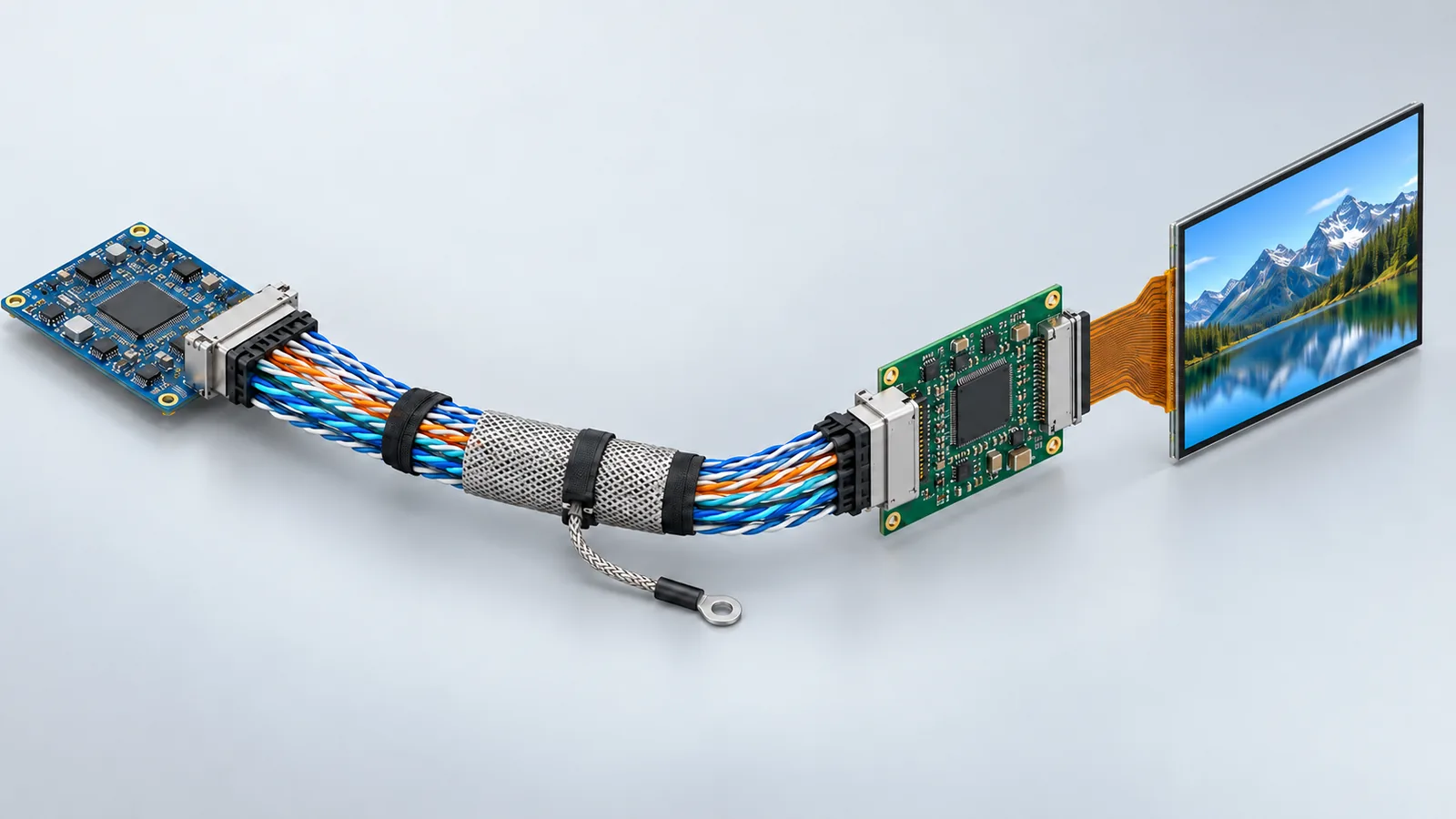
Keep the positive and negative conductors of each pair together through the cable and both connector transitions. Use a cable construction with controlled differential characteristics appropriate to the source and panel requirements. Avoid long untwisted breakouts, stubs, uncontrolled flat-cable sections and casual splices. PCB traces, connector, cable and receiver termination should be treated as one path.
Pair-to-pair skew and mapping
Confirm the clock pair, every data pair, pair polarity and bit mapping. Match electrical delay as required by the link budget, especially when multiple data pairs or dual channels are used. A mapping or polarity error can produce wrong colors, a split image or no image and cannot be fixed by shortening the cable.
Shielding and return paths
Shielding is a system decision. A shield can improve immunity and emissions only when its termination and chassis relationship are designed intentionally. Provide the required signal-ground or common reference conductors and keep the harness away from switching nodes, backlight converters, motors and relay wiring. Do not assume that adding foil or a braid automatically corrects a poor signal path.
Mechanical reliability
Respect the cable manufacturer’s bend radius. Keep repeated flexing away from rigid connector exits, add strain relief and check assembly tolerances. If the cable crosses a hinge or moving joint, it needs a flex-life requirement and a construction designed for that motion; an ordinary static LVDS harness is not automatically suitable.
A six-step cable-length selection workflow
- Freeze the electrical endpoints. Record the host or transmitter, TFT model, single/dual-channel mode, pixel clock, mapping, connector and pinout.
- Measure the installed route. Use the real enclosure and board locations. Include connector exit direction, bend radius and keep-out areas.
- Choose the shortest serviceable assembly. Add the minimum allowance needed for assembly, strain relief and maintenance; avoid stored cable loops.
- Define the complete cable. Specify pair construction, conductor size, shielding, drain/ground conductors, connector part numbers, pin map and acceptable tolerances.
- Build representative samples. Test the intended nominal length and, where production tolerance requires it, the longest permitted assembly.
- Qualify with margin. Validate image integrity, signal quality, EMC behavior and operation across the project’s voltage, temperature and noise conditions before releasing the drawing.
For a verified module example, see the DS-T070TISA-01 7-inch 1280×800 IPS LVDS TFT. Its published page helps with initial selection, while the current datasheet and controlled cable drawing remain necessary for cable approval.
How to validate the final LVDS link
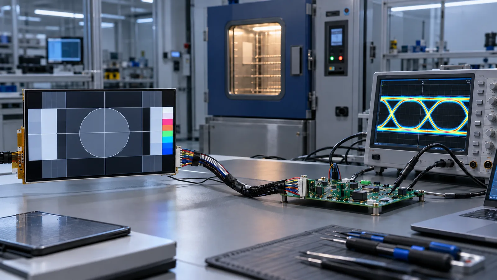
Run patterns that expose different fault modes: solid colors for mapping, gradients for bit errors, fine checkerboards and alternating pixels for high transition density, and moving content for intermittent faults. Cold start, warm operation and repeated power cycles should be included. Exercise the backlight and nearby loads in their worst normal operating modes.
Where access and equipment allow, inspect the differential waveform or eye at a suitable measurement point using probes and fixtures that do not dominate the result. Evaluate amplitude, crossing behavior, jitter and clock-to-data relationship against the transmitter and receiver requirements. An eye diagram is evidence about one test setup; it is not a substitute for validating the production assembly and environmental corners.
Common symptoms and likely checks
| Symptom | Check first |
|---|---|
| No image or unstable lock | Clock range, power sequence, channel mode, pinout, pair polarity and connector seating. |
| Wrong colors | LVDS bit mapping, color depth, pair order and polarity. |
| Left/right split or repeated content | Single/dual-channel configuration and odd/even pixel mapping. |
| Sparkles or intermittent lines | Cable loss, reflections, skew, connector quality, routing and receiver margin. |
| Failure near motors or converters | Harness route, common-mode path, shielding, grounding and conducted/radiated immunity. |
| Works warm but not cold, or vice versa | Clock and receiver margin, cable/connector variation and power sequencing across temperature. |
If the symptom is not clearly caused by cable length, follow the industrial TFT LCD interface troubleshooting workflow to separate power, reset, mapping, timing and signal-integrity faults.
What to send for an LVDS cable review
- Exact TFT module datasheet and model number.
- Host processor, graphics board or LVDS transmitter part number.
- Native resolution, target refresh rate and pixel-clock configuration.
- Single/dual-channel mode, bit mapping, connector part numbers and pinout.
- Required installed route, nominal length, tolerance, bend and motion requirements.
- Shield/ground concept, nearby noise sources and EMC requirements.
- Operating voltage and temperature range plus the planned validation method.
If the display is suitable but the connector, FPC or pin mapping differs, review the custom TFT LCD FPC and pinout guide. TFTWorks can then evaluate the display, cable and host-side constraints as one controlled interface.
Technical references
- Texas Instruments — LVDS Owner’s Manual: point-to-point topology, termination, controlled impedance and differential interconnect design.
- Texas Instruments — LVDS SerDes Gen I PCB and Interconnect Design-In Guidelines: cable, connector, skew, return-path and EMI considerations.
- Analog Devices — AN-1177 LVDS and M-LVDS Circuit Implementation Guide: why intended cable length should be tested in the application.