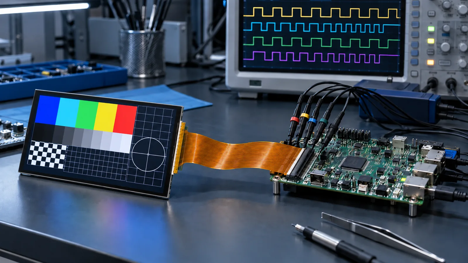
Parallel RGB—also called DPI, TTL RGB or dot-clock RGB in different ecosystems—sends pixel color data and timing signals directly from the host to the TFT LCD. Unlike a module with display RAM, a typical RGB panel depends on a continuous pixel stream. If the stream stops or its timing is wrong, the image can disappear, shift, roll, tear or show incorrect colors.
Start by checking that the host has a compatible LCD controller. If the available output is LVDS, MIPI DSI, MCU/SPI or HDMI, a bridge or a different module may be required. Use the RGB, LVDS, MIPI and MCU interface comparison before working on detailed timing.
Core RGB TFT LCD signals
| Signal | Purpose | Common integration risk |
|---|---|---|
| R[ ], G[ ], B[ ] | Parallel red, green and blue pixel values. | Wrong bit order, color depth or MSB/LSB mapping. |
| PCLK / DCLK | Pixel clock used to transfer or latch each pixel. | Wrong edge, frequency, duty cycle or excessive jitter. |
| DE | Marks the active region where RGB data is valid. | Wrong polarity or active width/height. |
| HSYNC | Defines horizontal line timing in sync-based modes. | Wrong pulse width, polarity or porch values. |
| VSYNC | Defines vertical frame timing in sync-based modes. | Wrong pulse width, polarity or vertical blanking. |
| RESET / STBY / DISP | Panel reset, standby or display-enable controls when provided. | Incorrect power sequence or logic level. |
| SCL/SDA or SPI control | Optional register initialization on some modules. | Assuming RGB timing alone completes initialization. |
How one RGB frame is organized
Each line contains an active pixel period plus horizontal blanking. Each frame contains active lines plus vertical blanking. The blanking interval is divided into a sync pulse, back porch and front porch. These intervals allow the panel’s internal timing to move from one active line or frame to the next.
Use the panel’s minimum, typical and maximum timing table. Do not calculate a pixel clock from active resolution alone because blanking pixels and blanking lines also consume clock cycles. Likewise, do not change porches merely to reach a familiar refresh rate unless the resulting values remain inside the panel specification.
An illustrative calculation
Suppose a hypothetical 800 × 480 panel configuration uses a horizontal total of 870 clocks and a vertical total of 494 lines. At 60 frames per second, the required pixel clock is:
This is a math example, not a setting for a particular TFTWorks module. Real Hsync, porch, Vsync, polarity and clock limits must come from the current datasheet for the selected display.
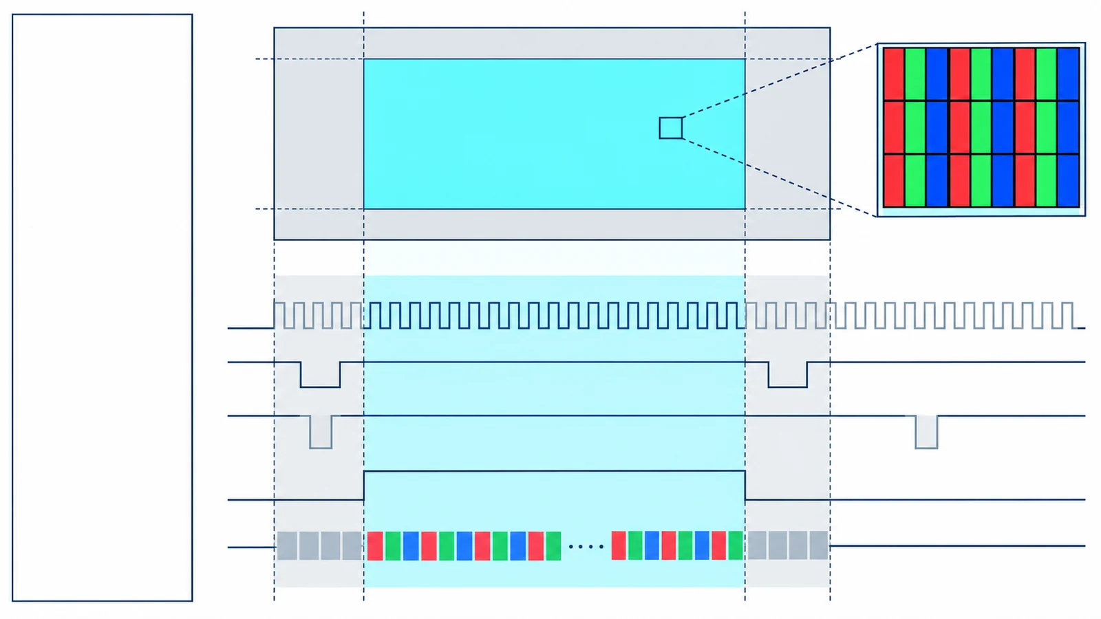
Pixel clock edge, setup time and hold time
The host must place stable RGB data around the panel’s sampling edge. The panel datasheet normally defines required setup and hold time relative to DCLK. The processor or display-controller manual defines its output timing. Board delay, connector loading, clock skew and signal quality consume the available margin.
If the panel samples on the rising edge, the host commonly changes data on the opposite edge to maximize stable time, but configuration labels vary. Verify the external pins rather than relying on a software option name. At higher clocks or longer routes, measure PCLK and representative data lines at the receiver side with a probing method suitable for the edge rate.
A nominal clock frequency inside the panel range does not guarantee compatibility. Check minimum high/low time, duty cycle, jitter and the source’s achievable divider error. The actual refresh rate may differ slightly from a round target when the clock generator uses integer or fractional dividers; keep all resulting values within both host and panel limits.
DE mode versus HSYNC/VSYNC mode
Some RGB panels primarily use DE to define the active rectangle. Others require HSYNC and VSYNC, and some support more than one mode. When DE is active, each PCLK transfers a valid pixel. Outside the active area, RGB values may be ignored, but blanking timing still has to satisfy the panel.
Do not assume that unused sync pins may be left floating. Follow the datasheet’s required mode, logic levels and pull configuration. When the host generates DE, HSYNC and VSYNC together, verify their alignment: the DE window must contain exactly the intended active width and height, with the specified porches relative to the sync pulses.
RGB565, RGB666 and RGB888 mapping
The format name states color resolution, not the connector pinout. RGB565 uses 5 red bits, 6 green bits and 5 blue bits; RGB666 uses 6 bits per color; RGB888 uses 8 bits per color. A module may expose 16, 18 or 24 data conductors, and the host controller may store pixels in a different memory format from the external bus.
Cross-reference every host output bit to the module pin. Preserve the intended most-significant color information when converting between widths, and follow the panel guidance for any unused inputs. A red/blue swap, inverted bit significance or shifted bus can still produce a recognizable picture, making mapping errors easy to misdiagnose as gamma or panel-quality problems.
Clock and memory bandwidth checks
The RGB wire rate is approximately the pixel clock multiplied by the number of active data lines, before considering simultaneous switching and control signals. Host memory traffic is a separate constraint. Framebuffer size depends on the stored bytes per pixel, which may differ from the external RGB width:
Double or triple buffering multiplies memory use. Compositing, rotation, scaling and graphics acceleration add read/write traffic. Confirm that the memory controller and DMA can feed the LCD controller without underflow while the CPU and other peripherals are active. An underflow can look like flicker, repeated lines or intermittent corruption even when the external timing registers are correct.
Common RGB timing risks and symptoms
| Symptom | Likely checks |
|---|---|
| Backlight on, screen blank | Panel power/reset, DE polarity, PCLK presence, required initialization and display-enable pins. |
| Image shifted or clipped | Hactive, Hsync, horizontal porches and DE alignment. |
| Image rolls vertically | Vactive, Vsync, vertical porches, frame rate and VSYNC polarity. |
| Wrong or swapped colors | R/G/B pin mapping, RGB565/666/888 format, MSB/LSB order and source pixel format. |
| Color banding | Actual bus width, dropped color bits, dithering configuration and framebuffer format. |
| Random pixels or edge noise | PCLK sampling edge, setup/hold margin, routing, ground return, drive strength and ringing. |
| Horizontal tearing | Framebuffer update synchronization, buffer switching and VSYNC handling. |
| Works only after reboot | Power rails, reset duration, initialization order and delay before starting PCLK/backlight. |
For a broader diagnostic sequence that also covers power, reset, connectors and host activity, use the industrial TFT LCD interface troubleshooting guide.
PCB and FPC considerations
Parallel RGB switches many single-ended lines together. Keep the display bus over a continuous reference plane, avoid split-plane crossings and minimize unnecessary vias and stubs. Control PCLK quality and route it away from noisy power nodes. Data-to-clock delay matching should be based on the real timing margin and edge rate rather than an arbitrary visual length rule.
The module FPC pinout controls connector location, contact side and bit mapping. If a standard module is otherwise suitable but the tail geometry differs, the TFT LCD FPC customization guide lists the drawing and pinout details to freeze before sampling.
Bring-up and validation sequence
- Confirm static facts. Match interface voltage, bus width, pinout, active resolution and all control pins.
- Program typical timing. Start from the panel’s recommended PCLK, sync, porch and polarity values.
- Verify the pins. Measure power, reset, PCLK, DE, HSYNC and VSYNC at the module connector.
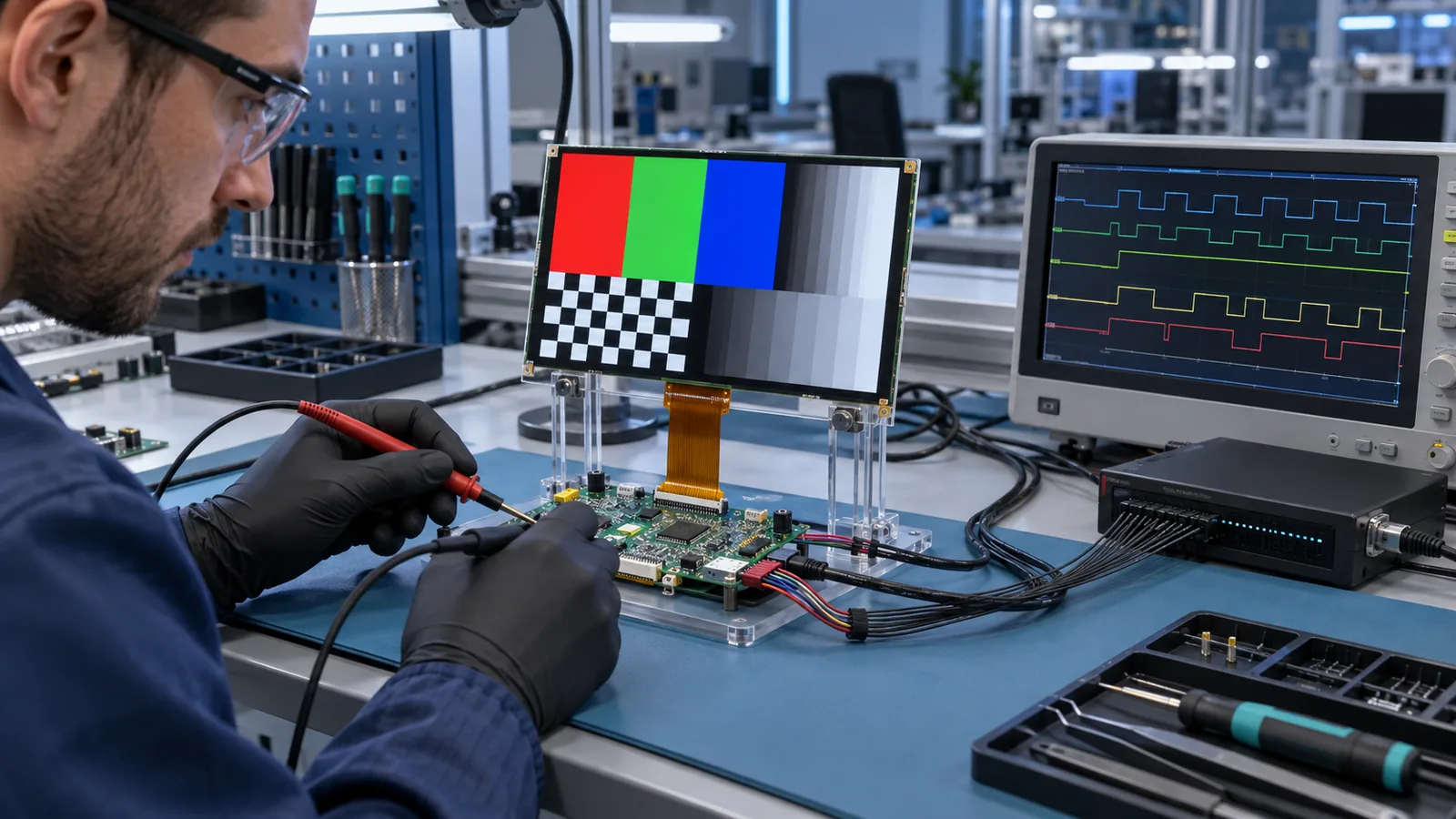
- Use diagnostic patterns. Display solid red/green/blue, gray ramps, one-pixel grids, checkerboards and moving content.
- Stress the data path. Run the rest of the system workload and watch for framebuffer underflow or contention.
- Test operating corners. Repeat cold start, warm operation, voltage limits and nearby switching-load tests required by the project.
- Freeze the configuration. Record the approved timing registers, clock source, pin map, initialization sequence and controlled drawing.
What to send for an RGB TFT compatibility review
- Exact TFT module model, current datasheet and mechanical drawing.
- Host processor or display-controller part number and I/O voltage.
- Resolution, target frame rate and available pixel-clock sources.
- RGB bus width, memory pixel format and complete connector pinout.
- HSYNC, VSYNC and DE mode plus required polarities.
- H/V active values, sync widths, front/back porches and allowed ranges.
- Reset, standby, serial initialization, backlight and power-sequence requirements.
- PCB/FPC route, cable length if applicable and environmental/EMC constraints.
Browse the TFT LCD interface selection page for verified RGB and LVDS module paths, or send the host and panel documents for a project-specific review.
Technical references
- NXP — i.MX RT eLCDIF RGB Mode Use Case (AN12302): RGB bus operation, programmable timing and total-width/height relationships.
- NXP — Different Display Configurations on the i.MX31 WinCE PDK (AN4041): HSYNC, VSYNC, DE, pixel-clock polarity and RGB data formats.
- Microchip — Graphics Suite Display Timing Guide: practical RGB display-controller timing configuration.