
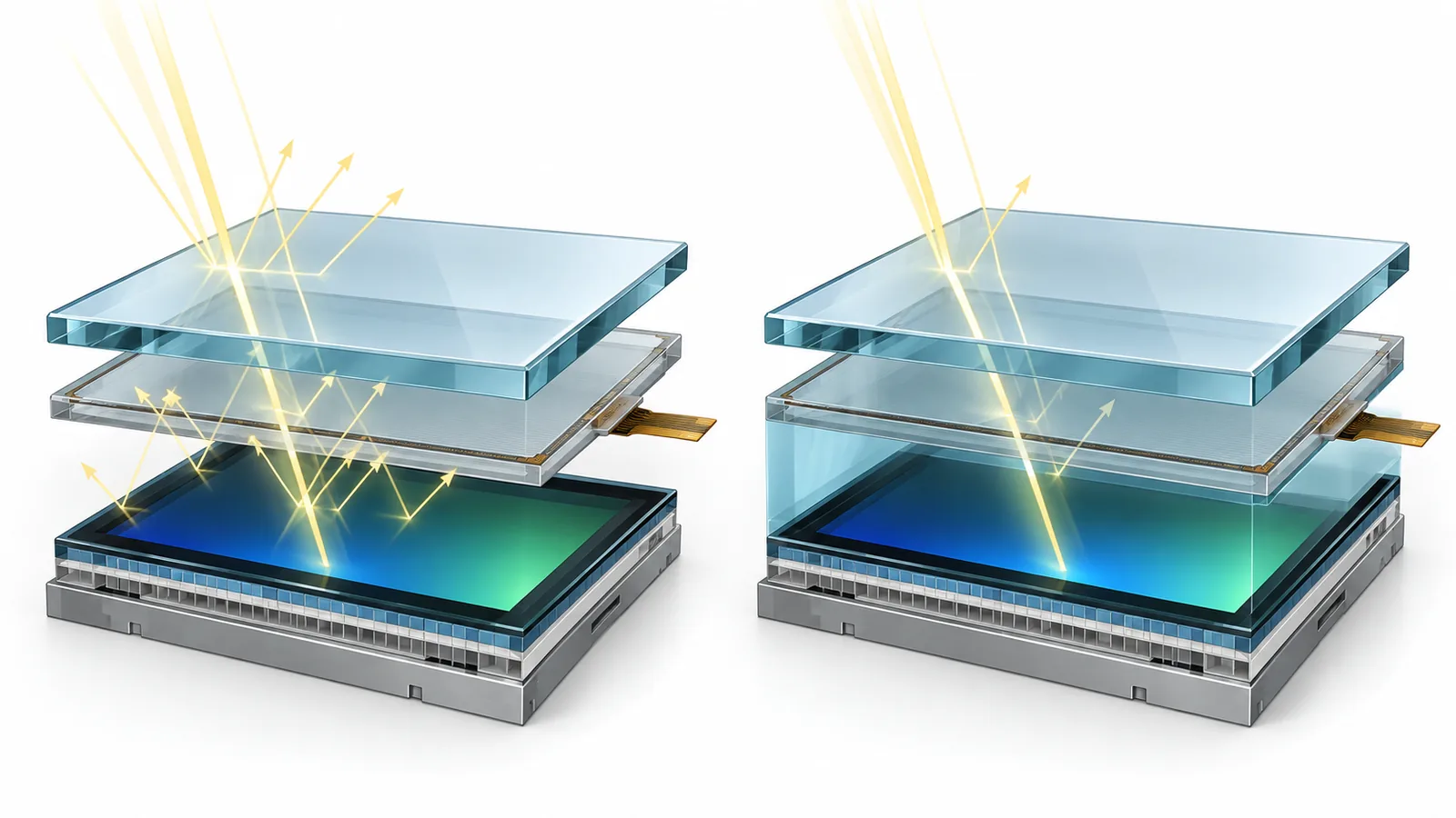
Many industrial displays place a touch panel or protective cover in front of the TFT. An air-bonded construction holds the layers together around the perimeter and leaves an internal air gap. An optically bonded construction fills that gap with an optically clear material and bonds the layers across the viewing area.
The decision is not simply “bonded is better.” Optical bonding changes optical behavior, mechanical stress, material compatibility, manufacturing yield, repair strategy and validation. Begin with the complete application requirement and use the sunlight-readable TFT LCD guide for the wider ambient-contrast context.
The short answer
Use optical bonding when reducing internal reflections, removing the air cavity, improving touch-to-image integration or strengthening the front stack delivers measurable value in the real application. Keep an air gap when the optical gain is unnecessary, field replacement is important or the cost, process and reliability risks of bonding are not justified.
What changes in a bonded TFT LCD stack?
Whenever light crosses between materials with different refractive indices, part of that light can be reflected. An air gap introduces additional optical boundaries between the LCD, air, touch panel and cover lens. Filling the gap with a compatible transparent material can reduce those internal reflections and allow more useful display light to reach the viewer.
The outermost cover surface still reflects ambient light. Optical bonding therefore does not replace an anti-glare or anti-reflective surface decision. Bonding addresses the internal gap; AG and AR address reflection behavior at treated surfaces.
Potential benefits for industrial equipment
Improved ambient contrast
Reducing internal reflections can improve the difference between displayed information and reflected surroundings, especially under bright factory lighting or outdoor ambient light. The gain must be measured on the finished assembly because cover treatment, touch electrodes, display luminance and viewing angle remain important.
No open air cavity between bonded layers
Filling the gap removes the cavity in which internal fogging or visible contamination could otherwise appear. This does not make the complete product waterproof. Edge sealing, enclosure gaskets, connectors, vents and housing design still determine environmental ingress protection.
More integrated touch and image plane
Bonding can reduce the visible separation between the touch surface and displayed pixels. That can improve perceived directness and reduce parallax in stylus or precision-touch tasks. Actual touch performance still depends on sensor design, controller tuning, cover thickness, grounding, water and glove requirements.
Mechanical support across the viewing area
A bonded stack can feel more unified and may improve resistance to some impact, vibration or surface-pressure conditions. It is not automatically stronger in every failure mode: adhesive modulus, glass thickness, frame support, thermal expansion and edge geometry affect stress transfer.
What optical bonding cannot fix
- It cannot compensate for a TFT backlight that is too dim for the required ambient condition.
- It does not remove reflection from the outer cover surface unless that surface also has a suitable treatment.
- It does not make an assembly waterproof, sunlight readable, vandal resistant or wide-temperature by label alone.
- It cannot correct an incompatible touch controller, excessive cover thickness or poor electrical grounding.
- It does not eliminate the need for enclosure-level thermal, EMC, optical and mechanical validation.
For outdoor projects, first select a realistic luminance class using the 800 vs 1000 vs 1200 nit TFT guide, then evaluate bonding and surface treatment within the same optical and thermal budget.
OCA vs LOCA/OCR: define the material and process
| Approach | General process characteristic | Design items to verify |
|---|---|---|
| OCA film or tape | Preformed optically clear adhesive laminated at a controlled nominal thickness. | Flatness, particle control, edge alignment, bubble removal, ink-step coverage, pressure and substrate adhesion. |
| Liquid optically clear adhesive or resin (LOCA/OCR) | Liquid material is dispensed, assembled and cured using a material-specific process. | Flow control, overflow, cure access and dose, shrinkage, edge containment, bubbles and material compatibility. |
The terminology varies by supplier, and neither approach is universally superior. Large size, cover curvature, border-print thickness, plastic outgassing, touch-sensor materials, production volume and available equipment can change the correct choice. Require the bonding supplier to define the approved material, process window and traceability.
Freeze these inputs during design review
- Layer stack: exact TFT, polarizer, touch sensor, cover material and any films or coatings.
- Controlled geometry: active area, viewing area, overall outline, black mask, adhesive coverage, edge clearance and total thickness.
- Surface and border: AG/AR/AF treatment, printed ink step, color, cure condition and acceptable edge appearance.
- Materials: adhesive family, nominal thickness, refractive behavior, UV/temperature/humidity resistance and compatibility with ITO, plastic and polarizer materials.
- Mechanical support: bezel pressure, gasket position, mounting torque, display frame and allowance for differential expansion.
- Touch requirement: controller, interface, cover thickness, gloves, water, stylus, grounding and EMC environment.
- Service strategy: whether the TFT, touch or cover must be replaceable separately and how valuable assemblies can be recovered.
Common bonding and reliability risks
Particles, voids, trapped bubbles, edge overflow, contamination, misalignment and incomplete cure can create immediate cosmetic defects. Later failures can include yellowing, haze growth, delamination, bubble formation, edge lift, visible mura or touch degradation after temperature, humidity, UV and mechanical exposure.
Plastic cover materials can outgas, and dissimilar layers expand differently with temperature. Thick printed borders require enough conformability or gap filling. A very stiff stack or poorly supported bezel can transfer stress into the LCD. These risks are why a material name or small-room-temperature sample is not sufficient evidence for an industrial release.
Validation before design release
- Approve the optical and mechanical stack drawing, material list and process revision.
- Inspect production-intent samples for particles, bubbles, edge quality, alignment and cosmetic defects under defined lighting.
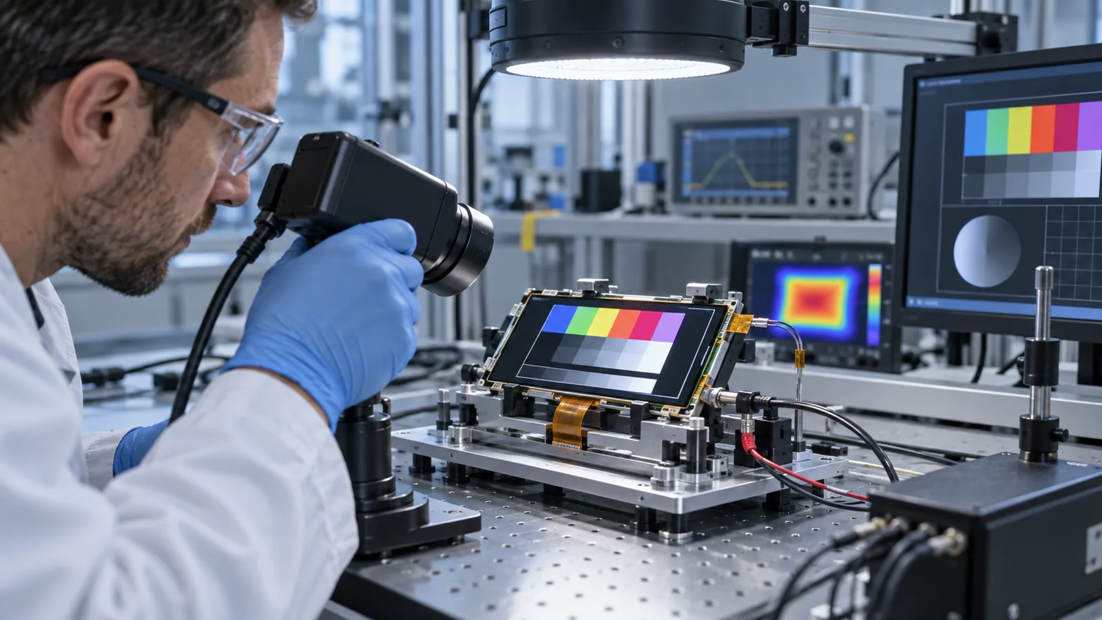
- Measure luminance, transmission or loss, reflection/ambient contrast, haze, clarity and color behavior as required by the project.
- Run touch tests through the final cover with required gloves, water, stylus and EMC conditions.
- Perform project-specific temperature, humidity, thermal-cycle, UV, vibration, impact and chemical-cleaning tests.
- Reinspect for delamination, bubbles, yellowing, mura, touch drift, seal damage and mechanical stress.
- Lock the approved sample, acceptance limits, material revisions and change-control process.
Current TFTWorks bonded-module paths
Current catalog examples include the DS-T043BPSA-02CP 4.3-inch 480×272 IPS module with PCAP and optical bonding, the DS-T050BWSA-02CP 5-inch 800×480 IPS module with PCAP and optical bonding, and larger 10.1-inch bonded PCAP configurations.
These pages are starting points, not universal bonded-stack specifications. Confirm the current datasheet, controlled drawing, cover construction, luminance definition, interface, operating range and sample configuration for the exact model. Browse TFT LCD modules with PCAP or send the required stack as a custom engineering request.
What to send for an optical-bonding review
- TFT model, datasheet and mechanical drawing.
- Touch type, controller, interface and operating requirements.
- Cover material, outline, thickness, black-mask drawing and surface treatment.
- Target bonding layers, total stack thickness and enclosure constraints.
- Ambient-light, luminance, operating/storage temperature and UV exposure.
- Required cosmetic, optical, touch, mechanical and environmental tests.
- Serviceability, change-control, sample quantity and volume assumptions.
Send the stack requirements for an engineering review. Mark unknown items explicitly so they become decisions or validation tasks rather than hidden assumptions.
Technical references
- EIZO — About Optical Bonding: explanation of the air gap, optical transmission, external-light reflection, durability and condensation considerations.
- 3M — Optically Clear Adhesive Technical Resources: OCA/LOCA process differences, plastic outgassing, bubbles, delamination and material compatibility.
- tesa — Optically Clear Adhesives: display-stack transparency, haze, adhesion, UV, heat and humidity design context.
- Henkel — Optical Bonding for Automotive Displays: LOCA materials, substrate combinations and light-curing process context.